
Design and construction of a functional FM receiver ensuring clear and stable radio signal reception. The project covers signal filtering, audio amplification, frequency synthesis, and FM demodulation.
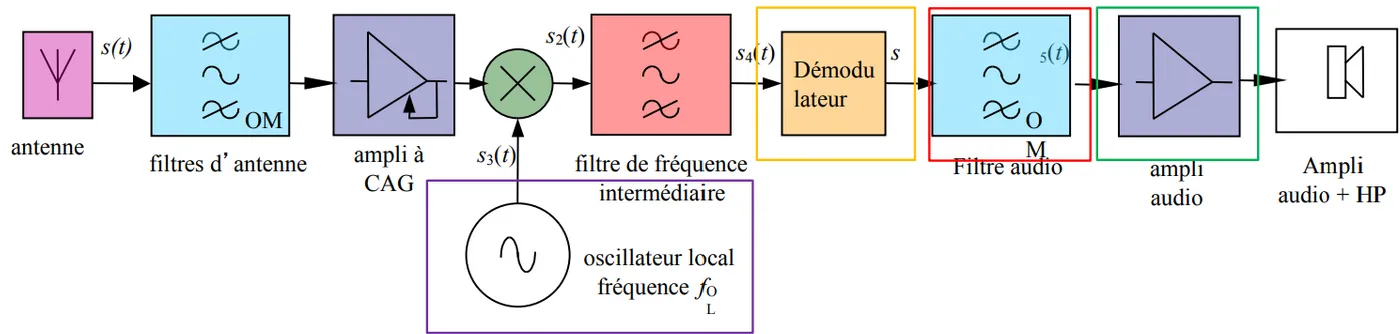
Figure 1 - General Principle of an FM Receiver
1. Audio Filtering
In order to obtain a good quality audio signal, we designed low-pass and high-pass filters that must respect several conditions:
We then find after normalization:
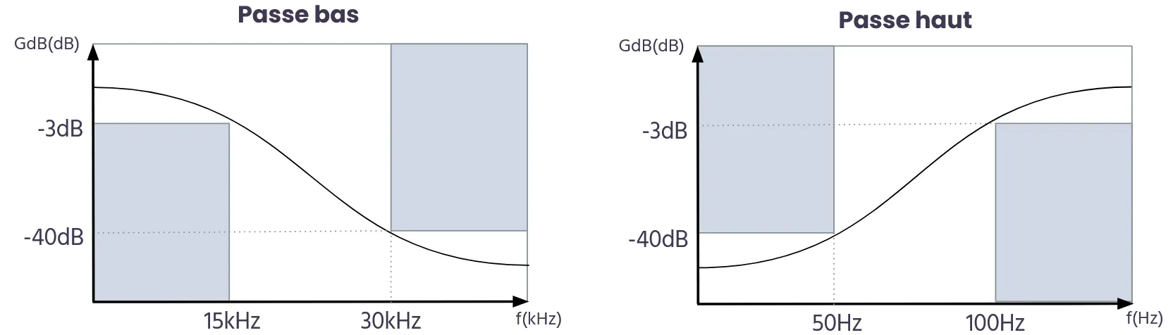
Figure 2 - Filter Specifications
The low-pass filter relies on a 4th order Chebyshev design, allowing attenuation of unwanted frequencies while maintaining a good response time.
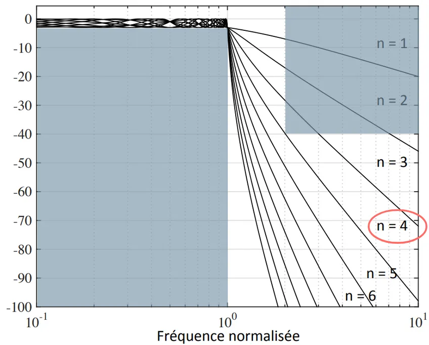
Figure 3 - 3 dB Chebyshev Filters
Which finally gives us:
After finding the exact values reported here for both cells, we can experimentally verify the correspondence with theory:
| Resistance | Theoretical | Normalized |
|---|---|---|
| R1 | 28kΩ | 27kΩ |
| R2 | 140kΩ | 130kΩ |
| R3 | 156kΩ | 160kΩ |
| R4 | 135kΩ | 130kΩ |
| Resistance | Theoretical | Normalized |
|---|---|---|
| R1 | 60kΩ | 62kΩ |
| R2 | 301kΩ | 300kΩ |
| R3 | 65kΩ | 70kΩ |
| R4 | 296kΩ | 300kΩ |
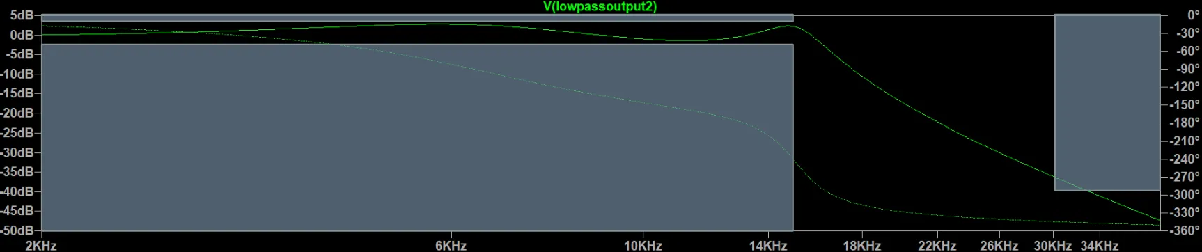
Figure 4 - Theoretical Representation
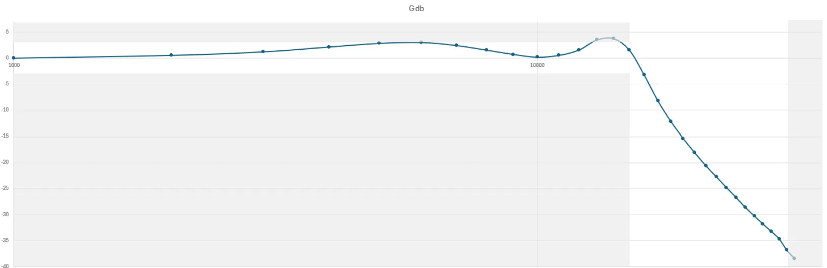
Figure 5 - Experimental Representation
As for the high-pass filter, it is based on a Rauch architecture repeated 4 times, ensuring effective suppression of parasitic low frequencies. We carefully calculated and normalized component values to ensure optimal frequency response.
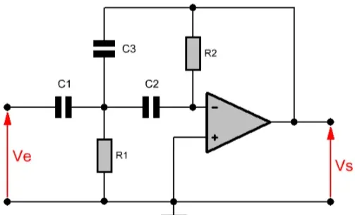
Figure 6 - Rauch Filter
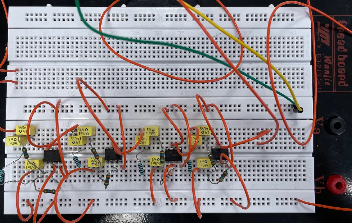
Figure 7 - Cascaded Filter Realization
Similarly, we can then calculate exact values for each component:
| Impedance | Theoretical | Normalized |
|---|---|---|
| R1 | 1kΩ | 1kΩ |
| R2 | 7.3kΩ | 7.2kΩ |
| C | 0.59μF | 0.56μF |
2. Audio Amplification
Once filtered, the audio signal must be amplified for quality sound reproduction. We adjusted the audio amplifier to obtain a maximum gain of 20 dB. A Noise Gate was integrated with a threshold set at 10 mVrms to attenuate unwanted background noise. The amplifier operation was configured via registers to optimize system performance:
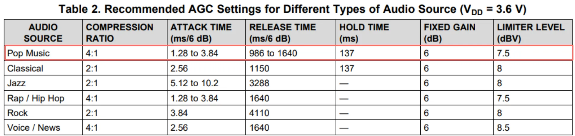
Figure 8 - Recommended Parameters Depending on Audio Source
This gives us the following information to enter as bytes in our module:
| Register | Byte |
|---|---|
| Register 1 | 11000011 |
| Register 2 | 00000001 |
| Register 3 | 00000110 |
| Register 4 | 00001010 |
| Register 5 | 00000110 |
| Register 6 | 01011100 |
| Register 7 | 00100010 |
3. Frequency Synthesis and Demodulation
To tune to the right radio station, we designed a frequency synthesizer. Starting from a quartz oscillating at 10.7 MHz, we calculated the necessary dividers and multipliers to capture the target frequency of Radio Campus (94.35 MHz). These parameters were implemented in an Arduino program allowing precise adjustment of the reception frequency. Here is an example of I2C configuration for the synthesizer:
#include <Wire.h>

#define SI5351_ADDRESS 0x60

void setup() {
    Wire.begin();
    Serial.begin(9600);

    // Frequency synthesizer initialization
    configureSynth();
}

void loop() {
    // The program loops without specific action after configuration
}

void configureSynth() {
    Wire.beginTransmission(SI5351_ADDRESS);

    // Example of synthesizer register configuration
    Wire.write(0x00); // Control register
    Wire.write(0x10); // Arbitrary value for init
    Wire.endTransmission();

    delay(100);

    Wire.beginTransmission(SI5351_ADDRESS);
    Wire.write(0x01); // Additional control register
    Wire.write(0x00); // Value to configure output
    Wire.endTransmission();

    Serial.println("Synthesizer configured successfully!");
}
The formulas used are as follows:
We finally find , which gives us the 3 sequences to transmit:
| Decimal | Binary | |
|---|---|---|
| M | 4000 | 111110100000 |
| K | 306905 | 1001010111011011001 |
| Latch | 884930 | 11011000000011000010 |
For this, we use a computer program again:
/// LATCH 1 : Calculation and decomposition
Latch1 = Mdiv * 4;
L11 = lowByte(Latch1);
L12 = highByte(Latch1);
L13 = 0;

Serial.print("Latch1: ");
Serial.println(Latch1);

/// LATCH 2 : Calculation and decomposition
K = ((Ndiv / 8) % 8192) * 256 + (Ndiv % 8) * 4 + 1;

L21 = lowByte(K);
L22 = highByte(K);
L23 = (K >> 16) & 0xFF;

Serial.print("Latch2: ");
Serial.println(K);

/// LATCH 3 : Fixed values
L31 = 0x82;
L32 = 0x80;
L33 = 0x0D;
We then used a phase-locked loop (PLL) to demodulate the FM signal. This approach allows extracting audio information contained in frequency modulation. A low-pass filter was designed to smooth the output signal and ensure faithful audio reproduction. After several tests and using the model chart, we adjusted component values to improve overall demodulator performance.
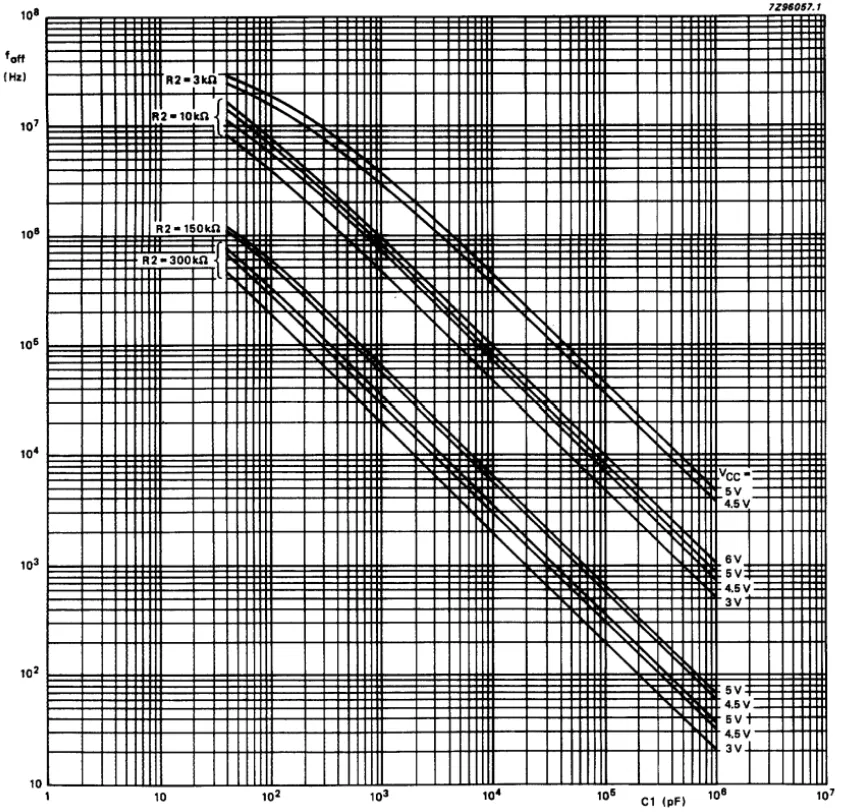
Figure 9 - Chart
Still according to the specifications, we have . This gives us, after experimental testing, the following final values:
- Potentiometer
4. LTSpice Simulation
Before physical implementation of the circuit, we performed validation by simulation under LTSpice. This simulation allowed us to verify the stability and frequency response of each receiver stage. Results confirmed good centering of the signal around 400 kHz, thus validating design choices made.
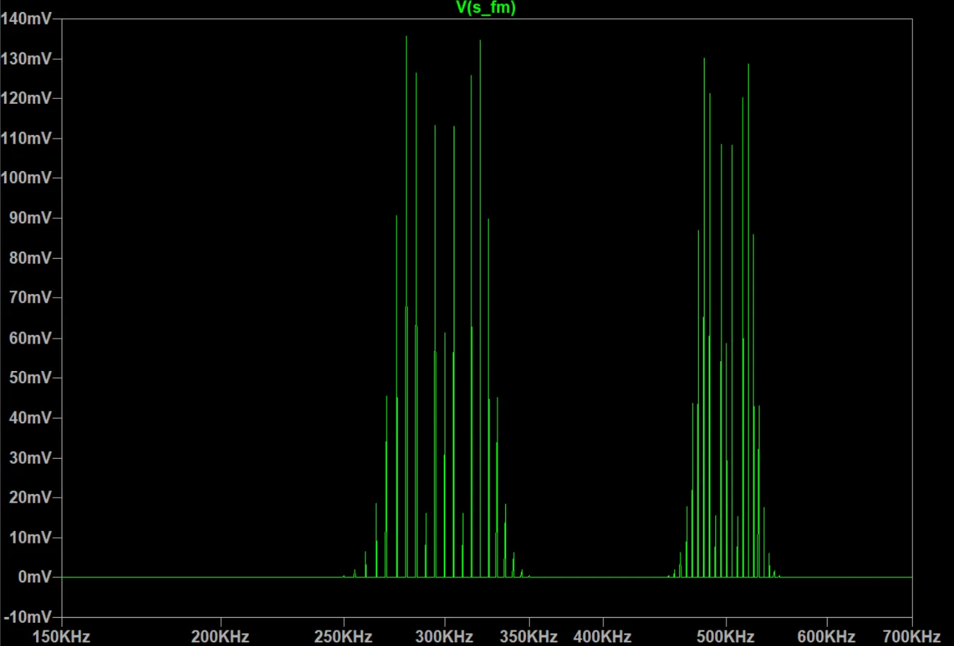
Figure 10 - LTSpice Simulation
Video 1 - Radio in action
This project might interest you
 2023
2023Design of an Active Noise Reduction System
Attenuating noise through phase opposition, from experimentation to Raspberry Pi.